Verify HDL Implementation of PID Controller Using FPGA-in-the-Loop
This example shows you how to set up an FPGA-in-the-Loop (FIL) application using HDL Verifier™.
The application uses Simulink® and an FPGA development board to verify the HDL implementation of a proportional-integral-derivative (PID) controller. In this example, Simulink generates the desired position of a motor and simulates the motor controlled by this PID controller.
Requirements and Prerequisites
Aside from the listed MathWorks products, other requirements include:
FPGA design software (Xilinx® ISE® design suite, Xilinx Vivado® design suite, Intel® Quartus® II design software, or Microchip Libero® SoC design software), with a supported version listed in FPGA Verification Requirements.
One of the supported FPGA development boards. For supported hardware, see Supported FPGA Devices for FPGA Verification.
For connection using Ethernet: Gigabit Ethernet Adapter installed on host computer, Gigabit Ethernet crossover cable.
For connection using JTAG: USB Blaster I or II cable and driver for Intel FPGA boards. Digilent® JTAG cable and driver for Xilinx FPGA boards.
For connection using PCI Express®: FPGA board installed into PCI Express slot of host computer.
Prerequisites:
MATLAB® and FPGA design software can either be locally installed on your computer or on a network accessible device. If you use software from the network you will need a second network adapter installed in your computer to provide a private network to the FPGA development board. Consult the hardware and networking guides for your computer to learn how to install the network adapter.
Set Up FPGA Development Board
Skip this step and step 2 if you are using PCI Express connection for simulation. If you have not set up your PCI Express connection, use the support package installation software to guide you through PCI Express setup.
Use the following steps to set up your FPGA development board.
Make sure that the power switch remains OFF.
Connect the AC power cord to the power plug. Plug the power supply adapter cable into the FPGA development board.
Connect the Ethernet connector on the FPGA development board directly to the Ethernet adapter on your computer using the crossover Ethernet cable.
Use the JTAG download cable to connect the FPGA development board with the computer.
Make sure that all jumpers on the FPGA development board are in the factory default position, except for Microchip PolarFire, which requires special settings. See Installing Microchip Polarfire Evaluation Kit.
Set Up Host Computer-Board Connection
Skip this step if you are using JTAG connection for simulation. For connection with Ethernet, you must have a Gigabit Ethernet network adapter on your computer to run this example.
On Windows®, do the following steps:
Open the Control Panel.
Type View network connections in the search bar. Select View network connections in the search results.
Right click the connection icon to your FPGA development board and select Properties from the pop-up menu.
Under This connection uses the following items, select Internet Protocol Version 4 (TCP/IPv4) and click Properties.
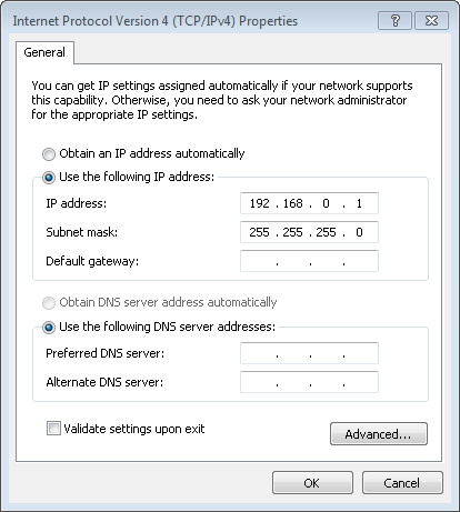
Select Use the following IP address:. Set IP address to 192.168.0.1. If this address is in use by another computer on your network, change it to any available IP address on this subnet, such as 192.168.0.100. This is your host computer address. Set the Subnet mask to 255.255.255.0. Your TCP/IP properties should now look the same as in the following figure:
On Linux®:
Use the ifconfig command to set up your local address. For example:
% ifconfig eth1 192.168.0.1
In this example, eth1 is the second Ethernet adapter on the Linux computer. Check your system to determine which Ethernet adapter is connected to the FPGA development board. The above command sets the local IP address to 192.168.0.1. If this address is in use by another computer on your network, change it to any available IP address on this subnet, such as 192.168.0.100.
Prepare Example Resources
1. Set Up FPGA design software
Before using FPGA-in-the-Loop, set up your system environment for accessing FPGA design software. You can use the function hdlsetuptoolpath to add ISE, Vivado, Quartus, or Libero SoC design software to the system path for the current MATLAB session. For information about supported versions of FPGA design software, see FPGA Verification Requirements. Example command lines for each tool are given below. Substitute with your actual executable if it is different.
For Xilinx FPGA boards using ISE design software, run:
hdlsetuptoolpath('ToolName','Xilinx ISE','ToolPath','C:\Xilinx\14.7\ISE_DS\ISE\bin\nt64\ise.exe');
For Xilinx FPGA boards using Vivado design software, run:
hdlsetuptoolpath('ToolName','Xilinx Vivado','ToolPath','C:\Xilinx\Vivado\2020.2\bin\vivado.bat');
For Intel boards, run:
hdlsetuptoolpath('ToolName','Altera Quartus II','ToolPath','C:\altera\20.1.1\quartus\bin\quartus.exe');
For Microchip boards, run:
hdlsetuptoolpath('ToolName','Microchip Libero SoC','ToolPath','C:\Microsemi\Libero_SoC_v12.0\Designer\bin\libero.exe');
2. Open the fil_pid model.
This model contains a fixed-point PID controller implemented with basic Simulink blocks. This model also contains a DC motor model controlled by this PID controller as well as the desired DC motor position as the input stimulus.
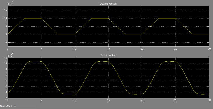
Run this model now and observe the desired and actual motor positions in the scope.

Launch FPGA-in-the-Loop (FIL) Wizard
To launch the FPGA-in-the-loop Wizard, select the Apps tab in the Simulink toolstrip and click HDL Verifier. This action adds the HDL Verifier tab to the Simulink toolstrip. Then, in the HDL Verifier Mode section, select FPGA-in-the-loop. Click Import HDL Files in the Generate FIL Block section.

Alternatively, you can enter the filWizard command at the MATLAB command prompt.
filWizard
Specify Hardware Options in FIL Wizard
Set the FIL options for the FPGA development board.
1. Specify if the wizard will generate a FIL Simulink block or a FILSimulation MATLAB System Object. For this example, select Simulink for FIL simulation with Simulink.
2. For Board Name, select the FPGA development board connected to your host computer. If your board is not on the list, select one of the following options:
"Get more boards..." to download the FPGA board support package(s) (this option starts the Support Package Installer).
"Create custom board..." to create the FPGA board definition file for your particular FPGA board (this option starts the New FPGA Board Manager).
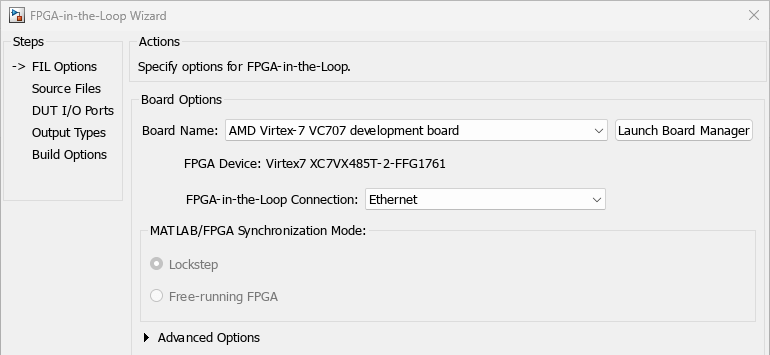
3. Select the connection for simulation. The available connection methods are Ethernet and JTAG. Not all boards support both connection methods.
4. Ethernet connection only: If you changed your computer's IP address to a different subnet from 192.168.0.x when you set up the network adapter, or if the default board IP address 192.168.0.2 is in use by another device, expand Advanced Options and change the Board IP address according to the following guidelines:
The subnet address, typically the first three bytes of board IP address, must be the same as those of the host IP address.
The last byte of the board IP address must be different from that of the host IP address.
The board IP address must not conflict with the IP addresses of other computers.
For example, if the host IP address is 192.168.8.2, then you can use 192.168.8.3 if it is available. Do not change Board MAC address.
To utilize BRAMs on the FPGA for buffering Ethernet packets, select Enable data buffering on FPGA.

5. Optional: If you would like to change the DUT clock frequency from the default (25MHz), you can expand Advanced Options and change the FPGA system clock frequency (MHz).
6. Click Next to continue.
Specify HDL Files in the FIL Wizard
Specify the HDL design to be implemented in the FPGA.
1. Click Add and browse to the directory you created in Prepare Example Resources.
2. Select these HDL files in the pid_hdlsrc directory:
Controller.vhd
D_component.vhd
I_component.vhd
These are the HDL design files to be verified on the FPGA board.
3. In the Source Files table, check the checkbox on the row of file Controller.vhd to specify that this HDL file contains the top-level HDL module.
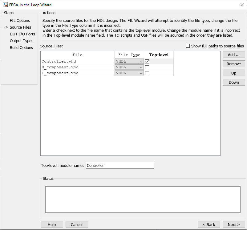
The FIL Wizard automatically fills the Top-level module name field with the name of the selected HDL file; in this case, Controller. In this example, the top-level module name matches the file name so that you do not need to change it. If the top-level module name and file name did not match, you would manually correct the top-level module name in this dialog.
Click Next to continue.
Review I/O Ports in FIL Wizard
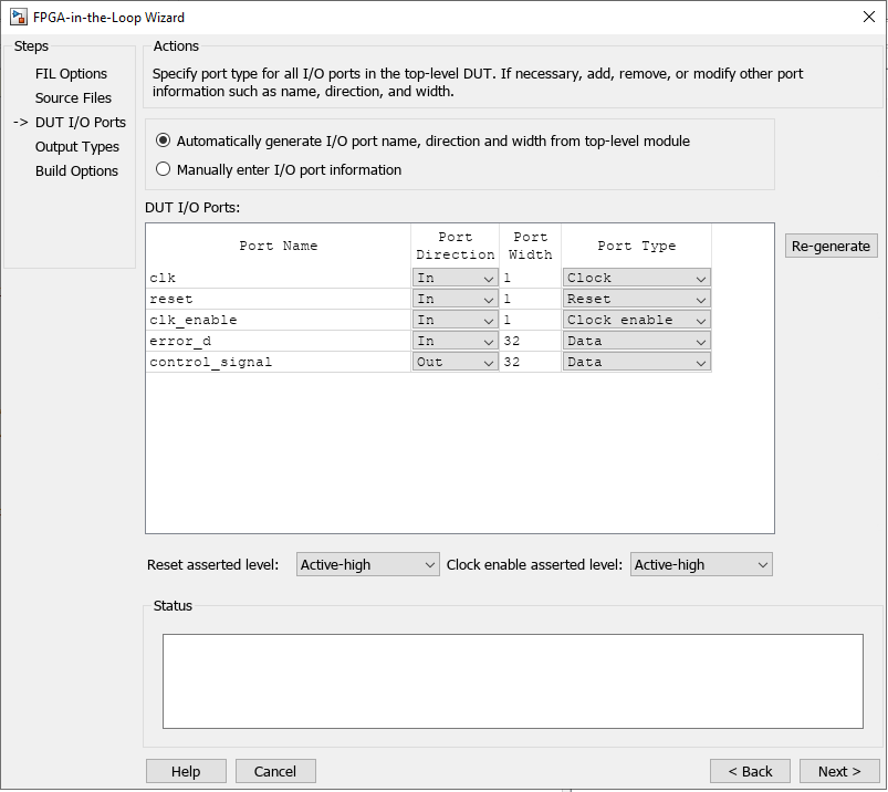
The FIL Wizard parses the top-level HDL module Controller in Controller.vhd to obtain all the I/O ports and display them in the DUT I/O Ports table. The parser attempts to automatically determine the possible port types by looking at the port names and displays these signals under Port Type.
1. Review the port listing. If the parser assigned an incorrect port type for any given port, you can manually change the signal. For synchronous design, specify a Clock, Reset, or Clock enable signal. In this example, the FIL Wizard automatically fills the table correctly.
2. Click Next to continue.
Set Output Data Types in FIL Wizard
1. For the HDL output control_signal change Data Type to Fixedpoint, Sign to Signed and Fraction Length to 28. This will makes the generated FIL block set the output signal of the FPGA design-under-test (DUT) to the correct data type.

2. Click Next to continue.
Review Build Options in FIL Wizard
1. Specify the folder for the output files. For this example, use the default option, which is a subfolder named Controller_fil under the current directory.
The Summary displays the locations of the FPGA project file and the FPGA programming file. You may need those two files for advanced operations.
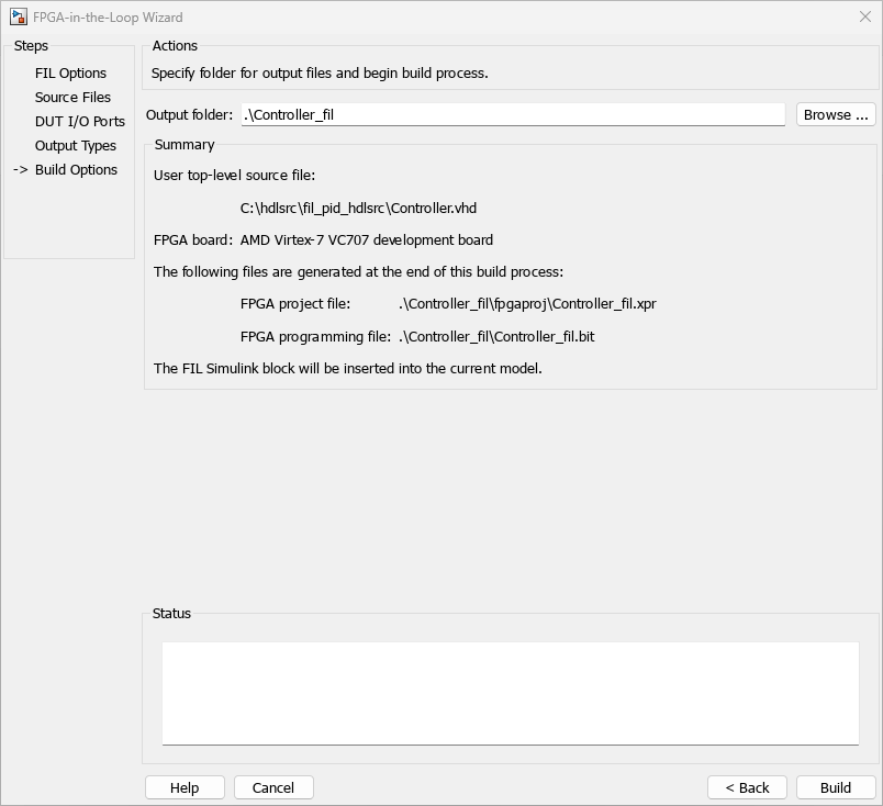
2. Click Build to start the build process.
During the build process, the following actions occur:
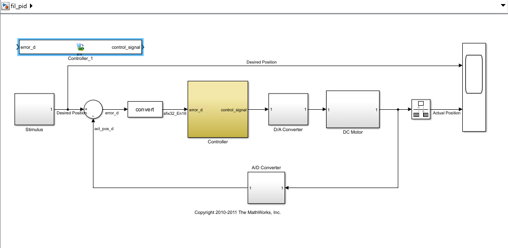
A FIL block named Controller is generated and inserted into the model as shown in the following figure.
After model generation, the FIL Wizard opens a command window where the FPGA design software performs synthesis, fit, place-and-route, timing analysis, and FPGA programming file generation.
When the FPGA design software process is finished, a message in the command-line window lets you know you can close the window. Close the window and proceed to the next step.

Set Up Model
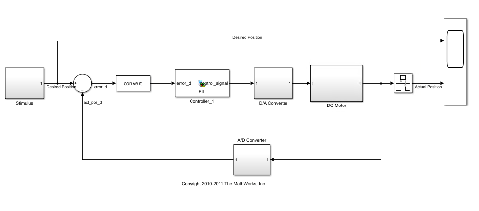
In the fil_pid model, replace the Controller subsystem with the FIL block generated in the new model. The modified fil_pid model now appears as shown in the following illustration:
Program FPGA
1. Switch FPGA development board power ON.
2. Double-click the FIL block in the fil_pid model to open the block mask.
3. In the opened block mask, click Load.
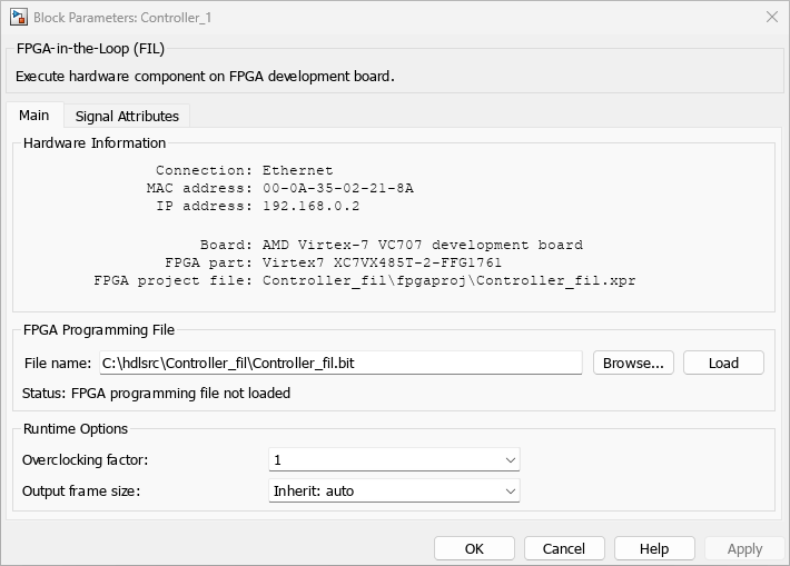
If your board is connected to the host computer through the JTAG cable properly, a message window displays to indicate that the FPGA programming file is loaded successfully. Click OK to dismiss this dialog.
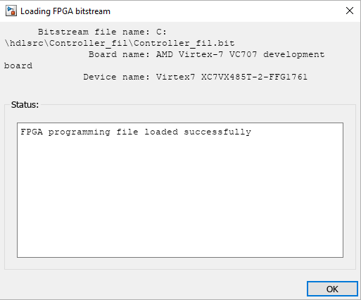
4. Ethernet connection only: You can test if the FPGA board is connected to your host computer properly through the ping test. Launch a command-line window and enter the following command:
C:\MyTests> ping 192.168.0.2
If you changed the board IP address when you set up the network adapter, replace 192.168.0.2 with your board IP address. If the Gigabit Ethernet connection has been set up properly, you should see the ping reply from the FPGA development board.
Review Parameters of FIL Block
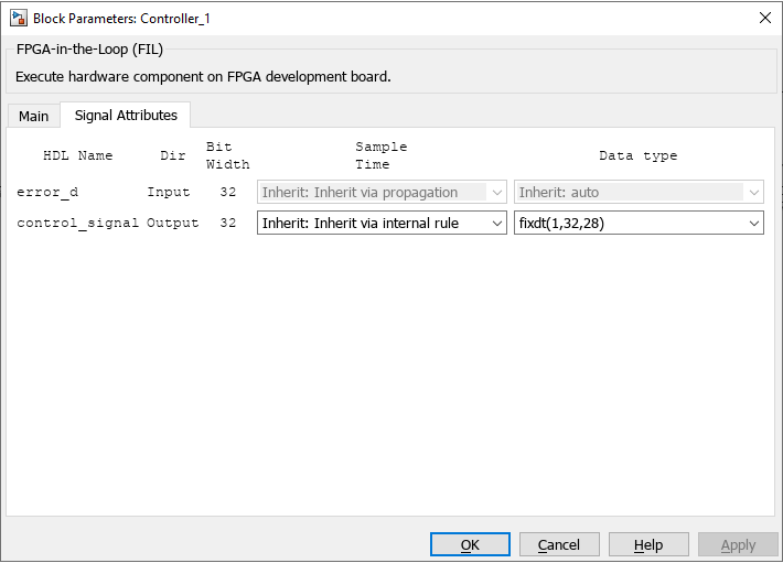
1. In the FIL block mask, click the Signal Attributes tab.
2. Verify that the Data Type of the HDL signal control_signal is fixdt(1,32,28). If it is not, change it.
3. Click OK to close the block mask.
Run FIL
1. Start simulation of the fil_pid model.
2. When the simulation is done, view the waveform of the desired and actual positions of the motor in the scope. Note that the results of FIL simulation should match those of the Simulink reference model that you simulated in Prepare Example Resources.
